SSW researchers are leveraging non-destructive methods, such as Micro-CT, to analyze and image sensitive electronics.
Integrated circuit (IC) micro-electro mechanical system (MEMS) chips are tiny electronic mechanical sensors and actuators that solve a wide variety of modern problems. Their utilization is very popular and their use is expanding with time:
Industries, such as aviation and defence, use only certified electronics because of their strict quality control. As these electronics age, ICs can become obsolete having no certified components available for direct replacement. Small shops (or ebay!) can be a source for IC replacements, but the internal dies need to be checked for compatibility since these parts are often uncertified and suspect. It is difficult to directly image the internal die since it is always encased in epoxy, but the die can be revealed by etching away the outer plastic casing (using nitric and sulfuric acid) in a process called “decapping”. Decapping obviously destroys the limited chips that are available, and is where micro-CT is beneficial. Micro-CT is a non-destructive technique that won’t damage the limited parts!
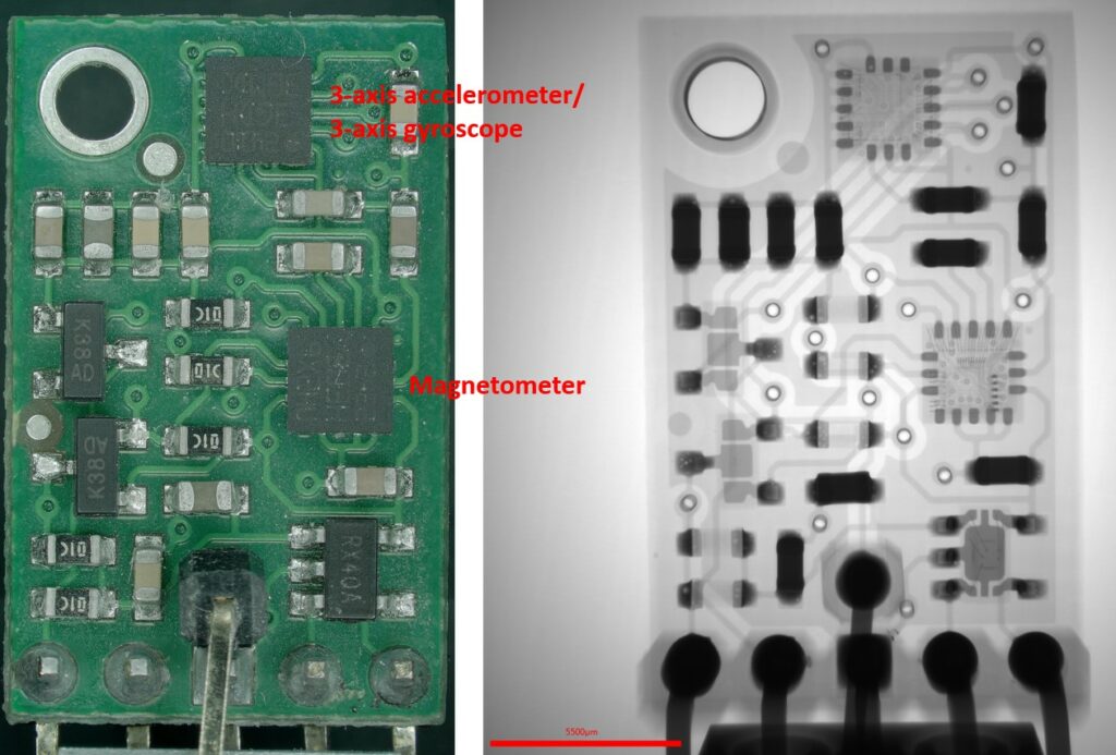
The left-hand image below is an optical image of a supplied PCB. The right image is an X-ray radiometric projection image of the PCB:
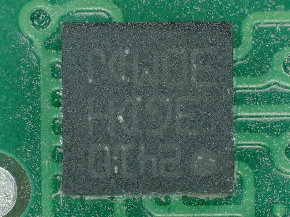
The image below shows chip that we investigated in detail (optically can only see the plastic black cap):
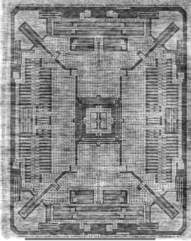
And with the magic of X-rays we see everything under the black cap in this 2D radiometric projection:
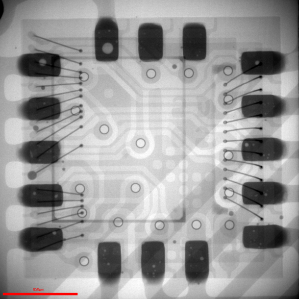
By using post-processing software to adjust a 2D X-ray tomography slice, we were able to observe the silicon die in the middle of the chip. The processed 2D X-ray tomography slice image below shows the MEMS silicon die that we found:
Our imaging showed that the IC components were stacked on top of each other in an arrangement called 3D-IC packaging. The video below shows the 3D-IC packaging that we found, along with the copper traces of the PCB and the silicon die:
Micro-CT is a great tool for analyzing and imaging electronics. We can use Micro-CT for solving a variety of issues including chip compatibility, fault finding of the bonding wires and solder points, and backwards engineering.