Cathode-Ray Tube TVs and computer monitors utilize a special electromagnetic phenomenon known as cathodoluminescence (CL) to produce visible light on a fluorescent screen. This technology’s use in modern computers and TVs has been gradually phased out in favour of LED technology, but interestingly this phenomenon has been utilized as a microscopic imaging technique.
The CL phenomena occurs when high-energy electrons, such as those produced during Scanning Electron Microscopy (SEM), are directed onto a CL-active insulating or semi-conducting material, and visible light photons are emitted. The emission of photons occurs due to the movement of electrons within the material’s electronic band structure, which includes both a valence band and a conduction band; the valence band has electrons and the lower energy conduction band has no electrons. Insulating and semi-conducting materials have an energy separation between the bands, and when high-energy bombarding electrons interact with the surface of the material, causing electron scattering events, some of the valence band electrons become excited, jumping up to the conduction band and leaving behind an electron hole in the valence band. It takes a lot of energy to keep an electron in the conduction band so it quickly falls back to the valence band to recombine with the hole. The energy difference between these electron states can be released in the form of a photon.
The materials exhibiting this phenomenon often contain defects within their crystal structure (defects such as impurities, dislocations, radiation damage, etc.), which can cause shifts to the wavelengths and energies of the photons. These shifted photons can be detected with a spectrometer or imaged as different colours or intensities of light.
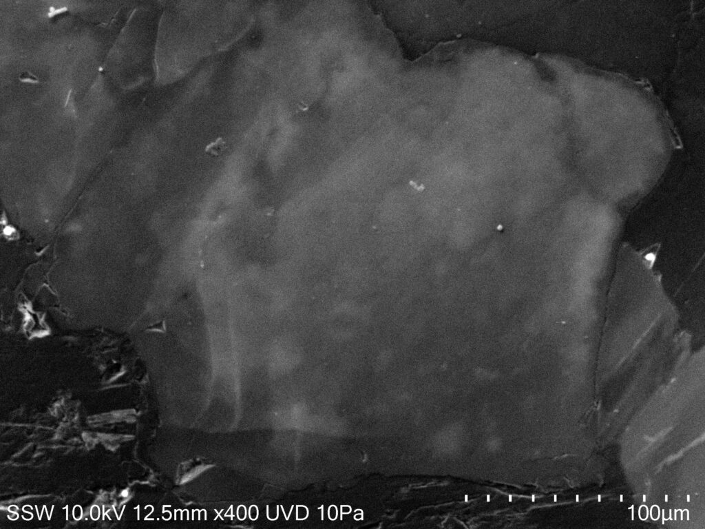
At SSW two of our SEM instruments are capable of CL imaging through Ultra Variable-Pressure Detectors (UVD). This detector contains a special scintillator, which is very sensitive to light and can be utilized to detect the light produced from CL-active materials. When imaging for CL using UVD, gas molecules are introduced into the SEM chamber through Variable Pressure (VP) mode, which amplifies the amount of light reaching the detector. If the UVD and VP mode are tuned correctly, stunning greyscale CL images of the material can be produced.
Some of the many materials that is technique can analyze include LED’s, nanoparticles, cement and other geological materials, optoelectronic and photovoltaic materials, phosphors, pharmaceuticals, and polymers.
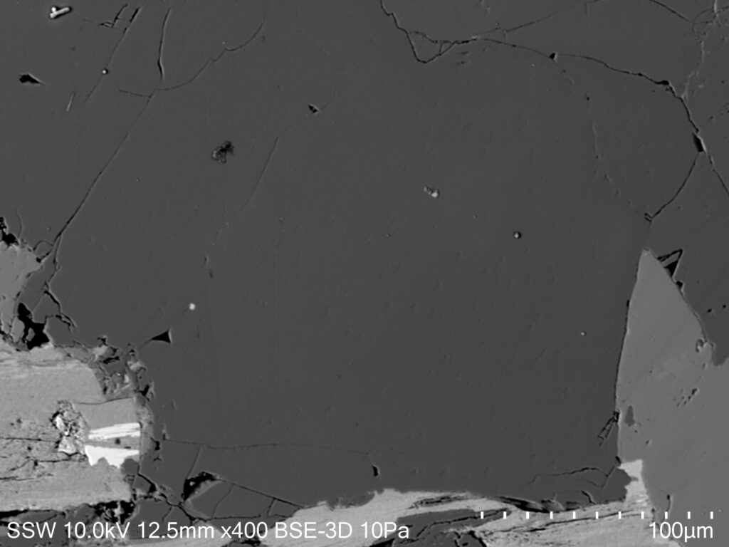
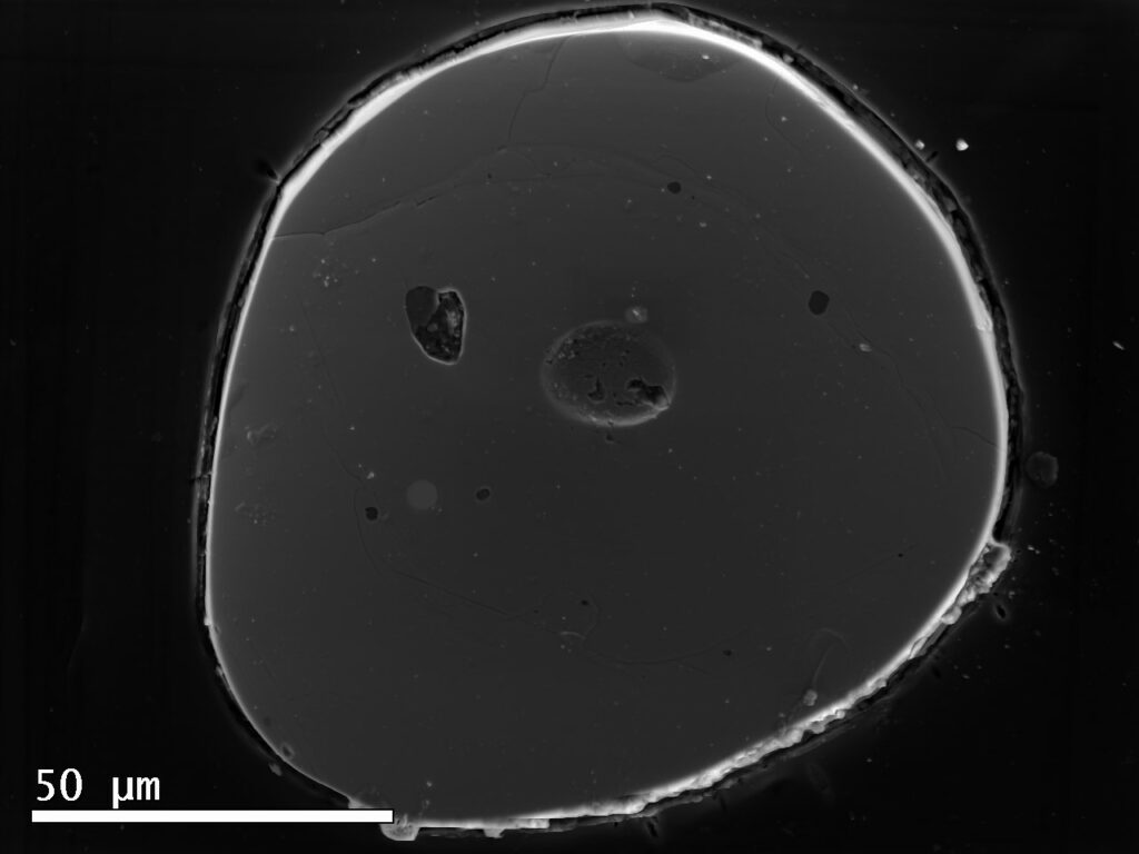
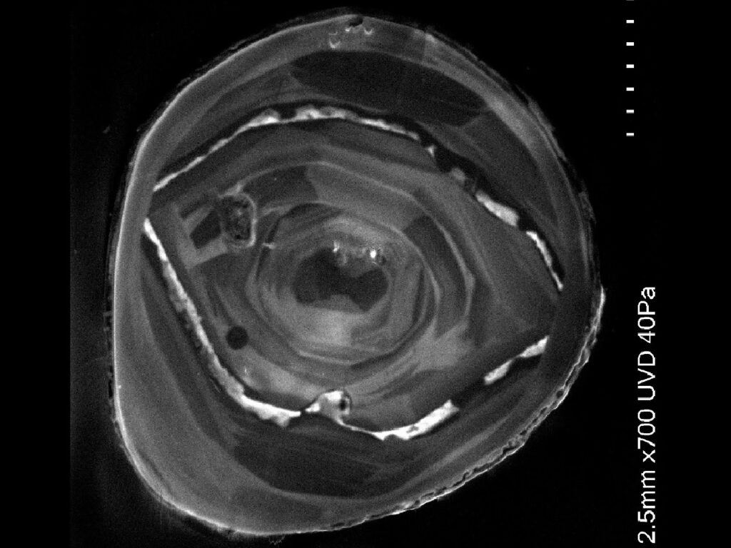
One example is the mineral zircon (ZrSiO4). Zircon can retain a rich geological record of the metamorphic, sedimentary and igneous processes that have happened over millions and billions of years (similar to how tree rings reveal a tree’s story over decades of time). The images below show a Secondary Electron (SE), traditional CL, and UVD-CL image of a sectioned zircon grain from the 616 Ma Artemisia Kimberlite pipe in Nunavut. The traditional CL and UVD-CL images reveal complex compositional zonation that is not visible in the standard SE image. These CL rings tell of a long geological history that can help with interpretations of the geological processes that occurred in the distant past and be used to guide future analyses.
(Image courtesy of ZAPLab at UWO)
UVD-based CL is another tool in SSW’s toolbox to help sort out the mysteries of the past, present and future. If you have a project that can utilize CL imaging, please don’t hesitate to let us know.